PS4 Aux Hax 2: Syscon
In the PS4 Aux Hax series of posts, we’ll talk about hacking parts of the PS4
besides the main x86 cores of the APU.
In this entry, we’ll recount some parts of the path taken to get permanent
arbitrary code exec on syscon.
Syscon recon
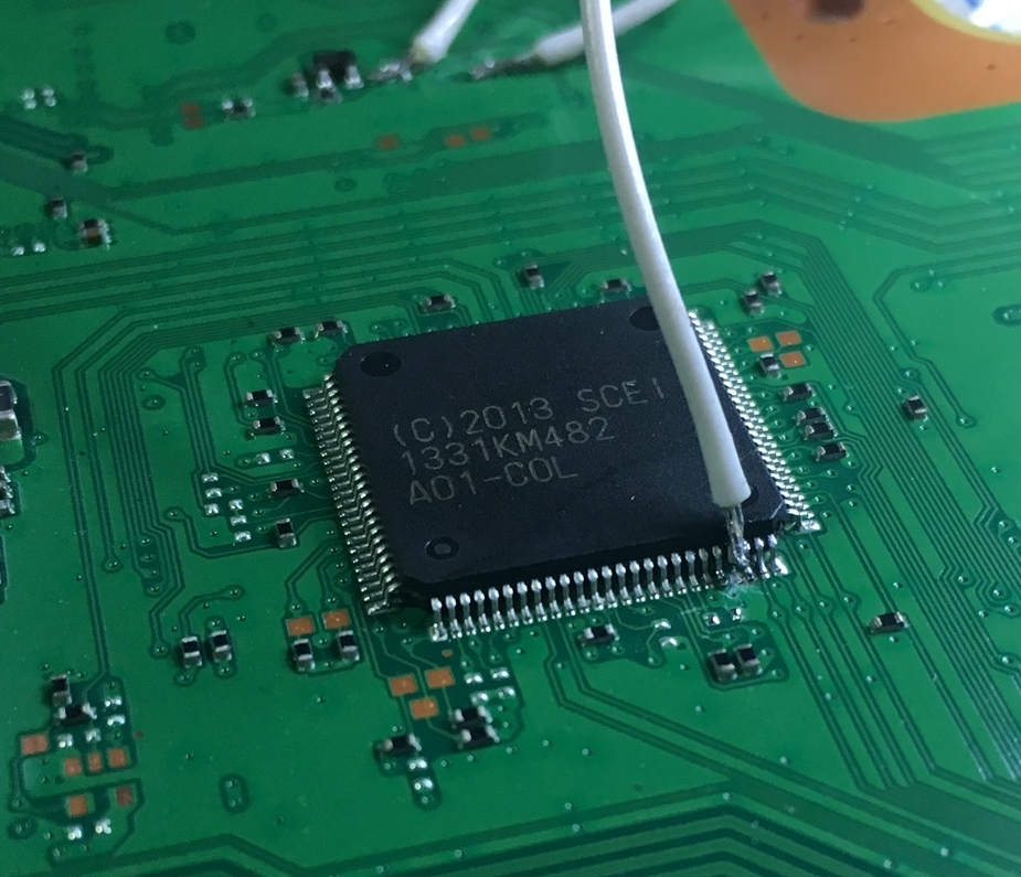
The “System Controller” appears as a mysterious “SCEI A01-C0L” device on SAA-001.
Thanks to droogie, we know this is a
rebranded Renesas RL78/g13
(specifically a R5F100PL on firmware v3.03).
After successful hax, we now know the internal name of syscon is “Colwick”.
The C in the model name is likely a reference to this.
Over time, the syscon has been revised with cost-reduced parts - however it is
still a RL78/g13.
Renesas offers a lot of information about the RL78 line of processors. Documentation and reference manuals can be found for software and hardware interfaces and there are various SDKs and libraries available.
Renesas provides target boards (i.e. the chip on a board with as little else as possible) for the RL78/g13. Unfortunately, I was not about to find a R5F100PL available in this configuration, however any model matching “R5F100xL” is very close to syscon, so I got the QB-R5F100SL-TB instead. Having a development board with the same architecture on hand will be useful for inspecting how built-in firmware (the “ROM” in this case) works. In addition, this gives a nearly identical platform to run arbitrary code on for the purposes of experimenting with power analysis and glitching - a capability which we lacked when dealing with Aeolia.
Another useful source of information about the workings of RL78 actually comes from old NEC documentation about the 78K0R, and Renesas documentation concerning porting codebases from 78K0R to RL78. The NEC architecture serves as the basis of RL78, and some registers/interfaces are not publicly documented for RL78, but are for 78K0R.
Please reference at least the beginning of the first part of this blog series, which gives an overview of the SAA-001 board.
As part of working with syscon, we created a RL78 processor module for IDA.
Do we even care about syscon?
It became obvious while reversing other parts of PS4 that flash internal to
syscon is used as a small region of nonvolatile storage for other components on
the system. The syscon-internal flash contains nvs and snvs regions which
are accessible via icc. Syscon runs icc over SPI (basically SPI + an interrupt
line). Note there are multiple other “nvs” regions kept in sflash and managed
by EMC, the syscon nvs is different; throughout the remainder of this post “nvs”
will refer to syscon’s nvs only.
nvs stores data such as some parameters to use while booting the APU, the board ID and other artifacts designed to be tied to a given board, but not really requiring security (in the sense that anything with icc access is able to read/write nvs).
snvs on the other hand, is used expressly by the security processor (SAMU) inside the APU. This data is arranged in 0x20 byte “sectors”, upon which XTS is used by SAMU (with XTS sector size = 0x200 bytes…), with a key only accessible by SAMU. So the actual data is opaque to pretty much everything outside SAMU. The communication between SAMU and snvs is additionally CMAC’d, so even though the traffic flows over icc and is thus easy to man-in-the-middle, any changes to requests to snvs or replies to SAMU will result in failed transfers. To protect against replay attacks at the icc level, nonces are used.
Clearly there is some interesting data being stored in snvs, and SAMU must trust this data to some extent. Since the use of CMAC entails there’s a shared secret in both SAMU and syscon, it becomes possible to at least replay old traffic, if the CMAC key can be extracted from syscon. From reversing x86 FreeBSD, we knew that SAMU stores system firmware version and manufacturing mode information in snvs (among other things). Therefor, being able to replay old snvs replies should allow downgrading firmware - a capability normally prohibited.
In addition to mediating access to internal storage, syscon also performs other interesting tasks such as clock/power management for pretty much everything on the board, booting most processors, and acting as a proxy to miscellaneous low-speed peripherals.
Apart from the PS4 implications, syscon is a kind of esoteric architecture, so it would be fun to investigate and try for a generic way to achieve code exec on this architecture.
Reversing the ROM
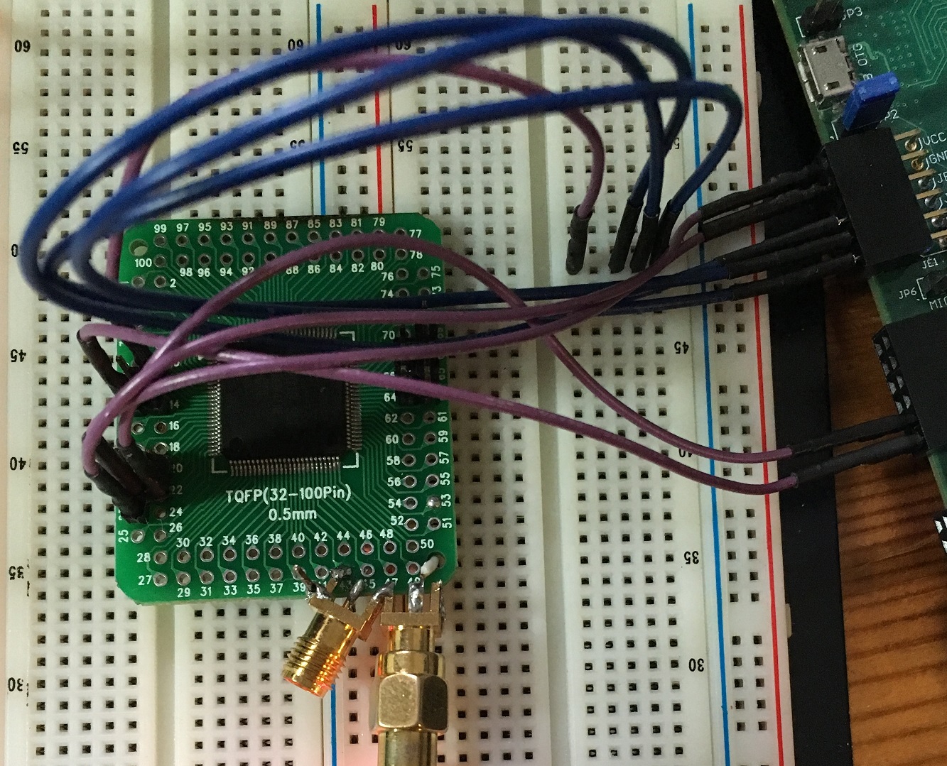
Using the target board and a debugger, it was trivial to extract the ROM from the device and begin reversing it. Since Renesas does not publicly document the debugger protocol (single-wire serial in the normal case), I traced the existing debugger I had, then reimplemented the protocol. This allowed using arbitrary host serial interfaces such as my own FPGA, simplifying integration with other tools.
RL78 security is mainly implemented in the form of a few bytes stored in a special region of internal flash. These bytes store a flag to indicate if debugging is disabled (OCDENSET), and an optional 10byte security key. The idea is that a programmer may set the key in order to limit debug access to authorized parties, and may program the OCDENSET bit to permanently disable debug access. The documentation also describes an OCDERSD bit, which indicates if failure to authenticate via the security key should cause the internal flash to be wiped or not. I found that the ROM does check this bit, but does not actually erase flash upon an error.
Even with debug functionality disabled (which offers SRAM read/write/exec functionality), a protocol to perform operations on flash (erase, program, checksum, etc.) via the serial interface also exists. The flash protocol has other lockdown mechanisms, which syscon does employ as well. However, there was still enough attack surface that I decided to reverse the entire ROM to see if there was some software bug allowing direct control, or perhaps a way to indirectly read out the flash (abusing the checksum function, for example). I found no abusable issues in the ROM, so again I turned to some hardware attack.
ROM glitchin’
Since the ROM code is known, it’s straightforward to search it for code sequences which would make good glitch targets. AFAIK the easiest glitch target is some form of a branch - and the most attractive code pattern is therefor an infinite loop which may be broken out of with a glitch. Going with this very simplistic view of glitch capabilities, I found a very nice target:
; in main()
ef371  call $!efbfe         ; tool_rx (read initial byte)
 set_tool_en_3a
ef374  mov  b, #58
ef376  cmp  a, #58          ; if (init_cmd==3a) TOOLEN=3a (one-wire uart)
ef378  bz   $ef389          ; set_tool_en
 set_tool_en_35
ef37a  mov  b, #53
ef37c  cmp  a, #0           ; if (init_cmd==0) TOOLEN=35 (two-wire uart)
ef37e  bz   $ef389          ; set_tool_en
ef380  cmp  a, #197
ef382  bnz  $ef382          ; hang if init_cmd!=c5
ef384  set1 ffe86.5         ; ffe86.5=1 (indicates OCD mode), TOOLEN not set
ef387  br   $ef391
 set_tool_en
ef389  mov  a, b
ef38a  mov  !f0080, a       ; TOOLEN
ef38d  set1 !f00a7.4        ; ??
ef391  call $!efba2         ; protocol_a_recv_cmd_soh
ef394  bc   $ef39f          ; reply if failed to recv cmd frame
ef396  cmp  !f0b00, #154    ; check for baudrate set cmd
ef39a  bz   $ef3a4          ; handle_buadrate_cmd
 reply_cmd_number_error
ef39c  mov  ffe4e, #4
ef39f  call $!efc8e         ; send_status_response_frame
ef3a2  br   $ef3a2
 handle_buadrate_cmd
ef3a4  mov  a, !f0b01
ef3a7  cmp  a, #4           ; assert baudrate <= 3
ef3a9  bnc  $ef3ce          ; reply_param_error_and_hang
ef3ab  or   a, ffe7d
ef3ad  mov  ffe7d, a        ; ffe7d |= baudrate
ef3af  mov  a, !f0b02
ef3b2  cmp  a, #18          ; assert voltage >= 1.8v
ef3b4  bc   $ef3ce          ; reply_param_error_and_hang
ef3b6  call $!ef791         ; handle_cmd_9a_baudrate_set
ef3b9  bf   ffe8a.1, $ef3c1 ; branch if fullspeed mode
ef3bd  mov  !f00f4, #128    ; RMC = 80      set wide-voltage mode
ef3c1  bf   ffe86.5, $ef3d6 ; if init_cmd!=c5, prepare for protocol A
ef3c5  bt   ffe81.7, $ef3f9 ; if OCDENSET==1, skip protoA init
ef3c9  mov  ffe4e, #16      ; (above branch not taken if OCD not allowed)
ef3cc  br   $ef3d1          ; send_reply (protect error)
 reply_param_error_and_hang
ef3ce  mov  ffe4e, #5
 send_reply
ef3d1  call $!efc8e         ; send_status_response_frame
 ; XXX hope if init_cmd==c5 && OCDENSET==0, can glitch past this hang, into ocd
ef3d4  br   $ef3d4
 setup_protocol_a
 ; ...execution continues, but ffe86.5 == 1, meaning OCD will be entered
Essentially the ROM will read the request to enter OCD (On Chip Debug) mode, see that OCDENSET indicates debugging is disabled, and fall into an infinite loop. Breaking out of this loop will resume the init process - OCD should continue as normal since no state was cleared during the failure handling.
It should be pointed out that the glitch method was dropping a voltage rail to
ground for a short period of time. The rail targeted is the core voltage
(R5F100PL has separated core/io rails). Since there were no real timing constraints
(just need to wait to ensure it has fallen into the infinite loop), this was
very easy to rig up. Eventually, this stage of the attack was actaully possible
to do in-circuit:
 ^ Vdd pin lifted, connected to glitcher. REGC capacitor removed. Serial and
reset are in the background.
^ Vdd pin lifted, connected to glitcher. REGC capacitor removed. Serial and
reset are in the background.
Are we there yet?
While breaking out of above infinite loop allows entering the OCD protocol command loop, we could not actually execute any useful OCD commands. From the errors generated, it was clear that the security key had been set in addition to OCD being disabled. On previous, similar ROMs, the security key was able to be read out via a timing side-channel. However, the v3.03 version of ROM in syscon appeared to be hardened against such an attack.
Time to find another glitch target, in the OCD command loop this time. The OCD dispatcher looks like the following:
handle_cmd_reset
 efe1f  bf  fffae.7, $efe1f ; while (MONSTA0.7 == 0) {}
 efe23  movw    ax, #833
delay_loop
 efe26  decw    ax
 efe27  cmpw    ax, #0
 efe2a  bnz $efe26        ; delay_loop
send_first_byte
 efe2c  clrb    a
 efe2d  set1    fffaf.6   ; ASIM.6 = 1
 efe30  clr1    fffaf.3   ; ASIM.3 = 0
 efe33  call    $!effa1   ; tool_tx(0)
read_cmd_loop
 efe36  mov a, !f0080     ; TOOLEN
 efe39  cmp a, #202
 efe3b  bnz $efe3b        ; if (TOOLEN != ca) { hang }
 efe3d  call    $!effb2   ; tool_rx
 efe40  mov x, a
 efe41  cmp0    a
 efe42  bz  $efe1f        ; handle_cmd_reset
 efe44  cmp a, #144
 efe46  bz  $efe76        ; handle_cmd_90
 efe48  cmp a, #145
 efe4a  bz  $efe82        ; handle_cmd_91
 efe4c  mov a, !f07f5
 efe4f  cmp a, #85        ; if (ocd_flag != 0x55)
 efe51  bnz $efe1f        ; handle_cmd_reset
 efe53  mov a, x
 efe54  cmp a, #146
 efe56  bz  $efe6a        ; handle_cmd_92
 efe58  cmp a, #147
 efe5a  bz  $efe6d        ; handle_cmd_93
 efe5c  cmp a, #148
 efe5e  bz  $efe70        ; handle_cmd_94
 efe60  cmp a, #149
 efe62  bz  $efe73        ; handle_cmd_95_97
 efe64  cmp a, #151
 efe66  bz  $efe73        ; handle_cmd_95_97
 efe68  br  $efe36        ; read_cmd_loop
The nice part of this is that ocd_flag (which is intended to be managed by
handle_cmd_91), is only checked once in the main loop when trying to execute
a command requiring authentication. If a glitch were able to invert the result
of the branch @ efe51, then we can bypass the ocd_flag check and execute a
single command. However, a single command isn’t enough to directly get arbitrary
code exec. The protocol expects an OCD client to upload code to main SRAM region,
then write a function pointer stored in SRAM, and then jump to the main SRAM
region by using the “exec” command to branch through the written function pointer.
Needing to glitch this loop 3 times in a row sounded painful, so I looked for a
workaround.
Firmware dumpin’
The workaround looked like so:
; tool_tx is @ effa1
; ocd_flag is @ f07f5
; base of this code is @ f07e0
    mov     es, #0
    movw    de, #0
next:
    mov     a, es:[de]
    call    !!0xeffa1
    incw    de
    movw    ax, de
    cmpw    ax, #0
    bnz     $next
    br      $after_ocd_flag
    nop
ocd_flag:
    .byte 0x55
after_ocd_flag:
    mov     a, es
    inc     a
    and     a, #0xf
    mov     es, a
    br      $next
This code is small enough to be written in a single command, and can be written
to f07e0, which is the default location the exec command will branch to. Also,
the ocd_flag is stored nearby, so we can modify the value such that the auth
check passes for the commands after the initial write. So, the flow is like:
- Glitch main loop to enter OCD loop
- Continuously try to issue the OCD write command to place our shellcode in SRAM
- While attempting to write shellcode, issue glitch pulses to perform initial auth bypass
- If write command returns success, it means the glitch worked, and we should now issue an exec command to jump to the shellcode
- The shellcode dumps flash memory out of the serial port continuously :)
Amazingly, this worked as well. At this time, I actually had syscon broken out
to simplify fiddling with it and debugging:
Finally, we got the full flash contents of syscon including keys used for firmware updates, snvs keys, and the RL78 security key. The RL78 security key is global across syscons, so once it’s known only the initial simple glitch is needed to get full OCD access. Knowledge of the firmware updates keys means we can encrypt and sign our own patch files (it’s not explained in depth in this blog post - but syscon on retail PS4s is locked down to only support patching, not full update images). Custom patches are still enough to introduce permanent code changes to syscon firmware without mucking around with glitching at all. Lastly, the snvs keys do allow downgrading the system firmware version (although there are some complexities involved).
We’ll leave you with a simple tool to extract nvs/snvs from a syscon image. The backing storage format seems to resemble storage formats used in other Sony “memory card” type of devices. A handy attribute of this format is that historical copies of data are kept for quite a long time.
Outtakes
Not seen here are the considerable other paths tried to get at the flash contents. Most were uninteresting and not fruitful, however one to highlight was CPA against the patch files. Key recovery of the encryption key was successful, however I got lost when attempting to recover the CMAC key. After inspecting the firmware code implementing the patch application process, it turned out the confusion was because the actual CMAC processing would only occur after issuing a soft reset to syscon - while I was expecting CMAC to be done directly after decryption. In fact, the activity observed in power traces (which I assumed was CMAC) was really the flash being erased and then having the intermediate patch data programmed into it.