PS4 Aux Hax 3: Dualshock4
In the PS4 Aux Hax series of posts, we’ll talk about hacking parts of the PS4
besides the main x86 cores of the APU.
In this entry, we’ll step outside of the PS4 itself, and take a look at pwning
the main handheld controller used by the system.
Pwn a controller, what?
The Dualshock4 initially came to my attention while looking through the x86 FreeBSD kernel. Parts of the driver stack used to communicate with peripherals are implemented in the kernel - even apart from the bluetooth/USB stacks upon which the functionality relies. In addition, the peripheral drivers track if each device has passed an authentication step or not (apparently to differentiate 1st-class peripheral citizens from lowly generic USB keyboards and such). Since this authentication involves verifying a RSA signature from the device, merely having a x86 kernel dump is not enough to exercise these code paths as there is no shared secret to use. I thought authenticated devices would allow access to a less picked-over kernel attack surface, so set out to acquire enough information from a peripheral such that I could authenticate with a real secret, and then run a fuzzer over the resulting communication channel. While I never got around to the fuzzer, I did pwn the controller with a technique that’s probably applicable to a wide range of FM3/FM4 microcontrollers.
Inspecting JDM-001
Some initial recon shows there are actually two different models (CUH-ZCT1U and CUH-ZCT2U), and at least ZCT1U has a few motherboard revisions under it’s belt. For similar reasons outlined in the first post in this series, I’ve picked the first revision to examine.
Nice motherboard pictures of some DS4 revisions were
already available.
Specfically we’re interested in JDM-001, which looks like this:
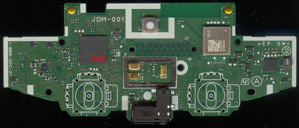
 It’s a bit hard to see here, but the main MCU is marked
 MB9BF002A - so it’s a
device in the
FM3 family
(which now belongs to Cypress). There’s an unpopulated header marked uP which
is probably used for debugging the MCU - the manuals for this processor family
indicate SWD is the supported debug interface. However I didn’t get any interesting
singals out of the uP header, and could not find a way to access the SWD interface.
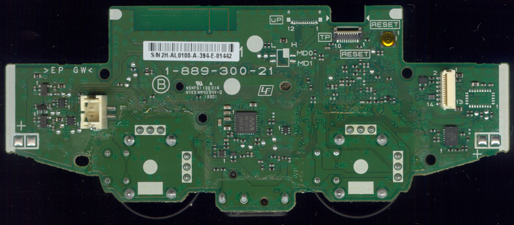
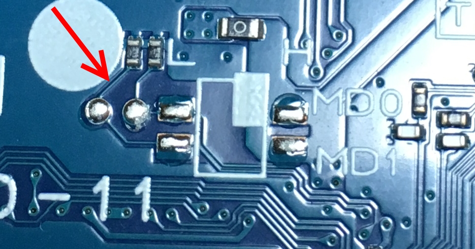
After digging through the manual some more, a section detailing MD0 and MD1,
which are marked on the board nearby uP, caught my eye:
| MD1 | MD0 | Operating Mode |
|---|---|---|
| - | 0 | User Mode Internal ROM (Flash Memory) Startup |
| 0 | 1 | Serial Writer Mode |
| 1 | 1 | Setting is prohibited |
Taking a closer look at JDM-001, it can be seen that both are pulled down (thus
it will boot from internal flash), and there’s obviously an unpopulated switch
of some type:
 After reading up on the serial programming mode, it became clear that this mode
must boot the MCU into some other part of the bootrom which then provides some
commands over serial or USB allowing flash access.
As a test, I tried toggling the MCU reset signal (also nicely labelled on the
board) with MD0 connected to the nearby Vcc. The DS4 did not resume gamepad
operation normally, and plugging it into a USB host showed a new USB descriptor.
After reading up on the serial programming mode, it became clear that this mode
must boot the MCU into some other part of the bootrom which then provides some
commands over serial or USB allowing flash access.
As a test, I tried toggling the MCU reset signal (also nicely labelled on the
board) with MD0 connected to the nearby Vcc. The DS4 did not resume gamepad
operation normally, and plugging it into a USB host showed a new USB descriptor.
Serial pwning mode
When looking into how USBDirect (the current offical flashing tool from Cypress)
worked, it could be seen initially transferring a code blob to SRAM and then
just communicating with that blob to actually interface with flash. This code
blob is what implements all of the useful functionality for flashing a device.
Luckily, an open source
replacement for this code blob
exists, so it’s quite easy to make modifications to the blob and hack around.
As the DS4 contains some cryptographic secrets, it’s understandably been locked down in an effort to prevent leaking the secrets out. And yet, we have the ability to freely load and execute any code in SRAM. It turns out the FM3 family implements flash read protection, which should keep the contents of flash secret even in these circumstances. According to the manual:
| Mode | MD | Chip Erase | Other Commands | Read | Access via JTAG |
|---|---|---|---|---|---|
| User | 00 | Enabled | Enabled | Valid data | Disabled |
| Serial | 01 | Enabled | Disabled | Invalid data | Disabled |
And so, as expected, attempting to simply read out the flash contents from the serial programming mode results in invalid data (all-0xff). Some other sneaky ideas were tried, like using DMA engines to access flash, etc. but nothing resulted in successful flash accesses.
Defeating read protection
While poking around in serial programming mode, it was observed that SRAM contents were actually kept across resets. This was easy to determine by filling SRAM with a pattern, resetting and re-entering serial programming mode, and then dumping SRAM. Even better, SRAM contents from user mode could be seen from serial programming mode. After staring at the dumps a bit, it was possible to determine where the firmware placed stacks, and from that, determine roughly where some function boundaries were. In fact, it probably would have been possible to get some keys just by scraping SRAM contents and looking for intermediate values. But we want easy mode (and all the keys)!
The SRAM persistence begs some questions: What other blocks in the MCU are not really reset when the reset signal is toggled? Can we influence execution of normal (“user mode”) execution from a previous serial programming mode session?
With a tip from [a hacker], we came across a nice feature which should come
standard with Cortex-M3 cores: the ARM Flash Patch and Breakpoint Unit (FPB).
Among the features of FPB is:
Six instruction comparators for matching against instruction fetches from Code space, and remapping to a corresponding area in System space.
This sounds perfect! We should just be able to plop our own code into SRAM, remap some code addresses in the protected firmware to our code in SRAM, then reset and allow the protected firmware to fall into our trap. Since we have stack dumps of the firmware, it was easy to guess an address to hook. The hook used just re-initialized serial programming mode, so existing code could be used to scoop out the flash.
As should be obvious, this idea worked - the state of the FPB unit persists across resets, even though the MD pins will be re-sensed (which is what allows executing the protected firmware without going through a full power cycle).